
CN-A・CN-K・CN-N
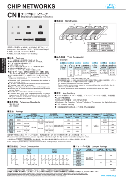
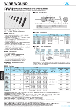
CHIP NETWORKS
EU
RoHS
CN-A・CN-K・CN-N
チップネットワーク
Chip Networks (Convex Termination)
■構造図 Construction
②
①
③
④
① 保護膜 ② 抵抗皮膜 ③ 内部電極 ④ 外部電極 ⑤ セラミック ⑤
外装色:黒、緑(CNZ1F8K)
Coating color:Black, Green(CNZ1F8K)
CN1H2N、CN1H4N、CN1E2K、CN1E4K、CN1FN8Kは無表示
CN1H2N、CN1H4N、CN1E2K、CN1E4K、CN1FN8K:No marking
ネットワーク抵抗器
Network Resistors
■特長 Features
●
●
●
●
●
●
●
●
●
●
●
●
●
●
●
●
●
●
チ
ップ抵抗より実装密度が向上する。
部
品搭載回数の減少による実装コストの低減。
は
んだフィレットの検査がしやすい。
2、4、8連の面実装抵抗アレイ。
±
1%に対応します。
実装時の画像認識が行いやすい。
(CN-K、CN-Nタイプ)
リ
フローはんだ付けに対応します。
端
子鉛フリー品は、欧州RoHS対応です。電極、抵抗、
ガラスに含まれる鉛ガラスは欧州RoHSの適用除外です。
A
(データ取得)
しています。
(CN1J4A, CN1J4K)
EC-Q200に対応
M
o r e a d v a n c e m e n t i n t h e m o u n t i n g d e n s i t y t h a n
individual chip resistors.
M
ounting cost reduction by decreasing the number of
parts mounting times.
E
asy soldering fillet inspection.
2
, 4 and 8 elements of SMD resistor arrays are available.
P
recision type ±1% is available.
S
uitable for an image recognition mounter due to square
corner design. (CN-K, CN-N type)
S
uitable for reflow soldering.
P
roducts with lead free termination meet EU-RoHS
requirements. EU-RoHS regulation is not intended for Pbglass contained in electrode, resistor element and glass.
A
EC-Q200 Qualified (CN1J4A, CN1J4K).
■参考規格 Reference Standards
Protective coating
Resistive film
Inner electrode
Outer electrode
Ceramic substrate
① 保護
② 抵抗
③ 内部
■品名構成 Type Designation
例 Example
CN
1J
品 種
Product
Code
形 状
Size
1H
1E
1J
2B
1F
4
1F8の表示
Marking
for 1F8
空欄:表示有り
Nil:Marking
N:無表示
N:No marking
K
T
TD
103
素子数
端子記号
端子表面材質 二次加工
Number of
Terminal
Terminal
Taping
Resistors
Surface Material
Symbol
2
A:凸型電極製品
T:Sn
TD:Paper
コーナー角無し (L:Sn/Pb※1) TE:Plastic
4
8
A:Convex type with
embossed
non-squared
BK:Bulk
corners
(Except 1H)
K:凸型電極製品
コーナー角有り
K:Convex type
with squared
corners
N:平型電極製品
コーナー角有り
N:Flat type with
squared corners
J
公称抵抗値 抵抗値許容差
Resistance
Nominal
Resistance Tolerance
F:4 digits
F : ±1%
J:3 digits
J :±5%
※1 1Hは端子表面材質記号としてTのみを対応致します。
※1 With type 1H, only the symbol T is available as the terminal surface material.
端子表面材質は鉛フリーめっき品が標準となります。
環境負荷物質含有についてEU-RoHS以外の物質に対するご要求がある場合にはお問合せください。
テーピングの詳細については巻末のAPPENDIX Cを参照してください。
The terminal surface material lead free is standard.
Contact us when you have control request for environmental hazardous material other than the substance specified by EU-RoHS.
For further information on taping, please refer to APPENDIX C on the back pages.
■用途 Applications
IEC 60115-1
JIS C 5201-1
●
●
デジタル回路のプルアップ/プルダウン抵抗
Resistors for Pull-up/Pull-down resistor for digital circuits.
■定格 Ratings
抵抗値範囲
抵抗温度係数
最高使用電圧 最高過負荷電圧 定格端子部温度 定格周囲温度 使用温度範囲
定格電力
T.C.R.
(×10−6/K)
Max. Working Max. Overload Rated Terminal Rated Ambient Operating Temp.
Power Rating Resistance Range(Ω)
Voltage
Voltage
Temp.
Temp.
Range
(W/Element)
F:±1% E24・E96 J:±5% E24 F:±1% E24・E96 J:±5% E24
CN1H2N
−55℃〜
0.031
—
—
12.5V
25V
—
CN1H4N
+125℃
10〜1M
CN1E2K
±200:R≧10Ω
25V
50V
CN1E4K
CN1J2K
0.063
10〜100k
+125℃
−55℃〜
±200:R≧10Ω
+70℃
+155℃
CN1J4A
±100:R≧10Ω ±400:R<10Ω
50V
100V
1〜1M
CN1J4K
CN2B4A
0.125
—
—
200V
400V
CN1F8K
10〜1M
—
−55℃〜
0.063※2
10〜100k
±200:R≧10Ω
25V
50V
CN1FN8K
+125℃
形 名
Type
テーピングと包装数/リール
Taping & Q'ty/Reel
(pcs)
TD
TE
10,000
—
10,000
—
10,000
—
10,000
—
5,000
—
5,000
—
5,000
—
—
4,000
5,000
—
定格電力で使用した場合、単一チップに比較し、発熱温度が高くなりますので御使用に際しましては御注意ください。
Please note that network resistors generate higher heat rather than single flat chip resistor even under rated power output.
R1
R2
※2 パッケージ当り0.25W 0.25W per package.
定格電圧は √ ̄ ̄ ̄ ̄ ̄ ̄ ̄ ̄ ̄
定格電力×公称抵抗値による算出値、又は表中の最高使用電圧のいずれか小さい値が定格電圧となります。
Rated voltage= √ ̄ ̄ ̄ ̄ ̄ ̄ ̄ ̄ ̄ ̄ ̄ ̄
Power Rating×Resistance value or Max. working voltage, whichever is lower.
■回路構成 Circuit Construction
R
R
1
CN1H2N, CN1E2K, CN1J2K
R1
CN1H4N, CN1E4K, CN1J4A
CN1J4K, CN2B4A
R1
R2
R1=R 2
R1
R2
R3
R1
2
R2
R3
R2
R3
■ジャンパー定格 Jumper Ratings
R4
CN1F8K, CN1FN8K
R4
R1
R2
R3
R4
R5
R6
R7
R8
R1=R 2=R 3=R 4 R 1 =R 2=R 3=R 4=R 5=R 6=R7=R8
あ1
R4
R1
R2
R3
R4
R5
R6
R7
R8
形 名
Type
CNZ1H2N
CNZ1H4N
あ1
CNZ1E2K
あ1
CNZ1E4K
CNZ1J2K
CNZ1J4A
CNZ1J4K
CNZ2B4A
CNZ1F8K
抵抗値
Resistance
定格電流
最大サージ電流
Current Rating Max. Surge Current
−
50mΩ以下
50mΩ max.
2A
1A
あ1
本カタログに掲載の仕様は予告なく変更する場合があります。ご注文およびご使用前に納入仕様書で内容をご確認ください。
車載機器、医療機器、航空機器など人命に関わったり、あるいは甚大な損害を引き起こす可能性のある機器へのご使用を検討される場合には、必ず事前にご相談ください。
Specifications given herein may be changed at any time without prior notice. Please confirm technical specifications before you order and/or use.
Contact our sales representatives before you use our products for applicationsあ1including automotives, medical equipment and aerospace equipment.
Malfunction or failure of the products in such applications may cause loss of human life or serious damage.
あ1
0.5A
Oct. 2014
www.koanet.co.jp
t
d
a2
c
a
b
P
d
c
t
W
b
P
W
した
あ1
d
c
d
うえ
a
d
c
c
d
まん中
CN1H4N
d
c
P
0.15±0.1
0.35
0.3±0.1
−
−
(0.5)
0.55
0.6±0.08 0.1±0.08 0.2±0.08
0.35
0.2±0.1
−
−
(0.4)
0.97
−
0.17±0.05
(0.67)
1.2
0.15±0.1
(0.5)
2.4
0.6±0.1
0.15±0.1
0.8±0.1
CN1H4N
(0201×4)
1.4±0.1
あ1
CN1E2K
(0402×2)
1.0±0.1
あ1
1.0±0.1
0.15±0.1 0.25±0.1
0.35
0.33±0.1
CN1E4K
(0402×4)
2.0±0.1
1.0±0.1
0.15±0.1 0.25±0.2
0.35
0.3±0.15 0.4±0.15
CN1J2K
(0603×2)
1.6±0.15
1.6±0.15
0.3±0.2
0.25±0.1
0.5
0.6±0.15
−
0.3±0.1
(0.8)
4.72
CN1J4A
(0603×4)
3.2±0.15 1.6±0.15
0.3±0.2
0.25±0.1
0.5
0.5±0.15
−
0.3±0.1
(0.8)
7.5
CN1J4K
(0603×4)
3.2±0.15 1.6±0.15
0.3±0.2
0.25±0.1
0.5
0.5±0.15 0.65±0.15 0.3±0.1
(0.8)
CN2B4A
(1205×4)
5.1±0.2
3.1±0.2
0.5±0.2 0.35±0.15
0.55
0.8±0.2
−
0.45±0.1
(1.27)
32.2
CN1F8K
CN1FN8K
(0602×8)
3.8±0.1
1.6±0.1
0.3±0.1
0.45
0.3±0.1
−
(0.15)
(0.5)
8.6
d
c
d
定格電力比(%)
Percent rated power
t
L
c
c
d
d
CN1H2N
CN1H4N
CN1F8K
t
c
c
d
d
まん中
L
0P
-0
d
-20
c
-40
-55
+20
+40
+60
+80
+100 +120
+70
周囲温度 Ambient temperature(℃)
W
+140
+125
+160
+155
d
c
d
d
W
c
c
40
20
-40
-20
-0
+20
+40
+60
+80
+100 +120
+70
+140
+125
端子部温度 Terminal part temperature(℃)
+160
+155
上記の端子部温度以上で使用される場合は、負荷軽減曲線に従って定格電力を
軽減してご使用ください。
※ご使用方法につきましては巻頭の“端子部温度の負荷軽減曲線の紹介”を参照
願います。
For resistors operated terminal part temperature of described for each size or
above, a power rating shall be derated in accordance with derating curve.
※Please refer to“Introduction of the derating curves based on the terminal
part temperature”on the beginning of our catalog before use.
■性能 Performance
規格値 Performance Requirements
ΔR±%
試験項目
Test Items
CN1E2K
CN1E4K
CN1J2K
CN1J4A
CN1J4K
60
-55
a
周囲温度70℃以上で使用される場合は、上図負荷軽減曲線に従って、定格電力
を軽減してご使用ください。
For resistors
operated
at an tambient temperature of 70℃ or above, a power rating
P
a
shall be derated in accordance with the derating curve.
L
80
0
-60
t
-60
0.3±0.1
7.5
100
40
L20
Weight(g)
(1000pcs)
CN1H2N
(0201×2)
d
d
a2
cb
c
c
aa
b
( )内の数値は参考値です。 Figures in parenthesis are referential values.
CN1E2K
CN1E4K
あ1
CN1J2K
CN1J4A
CN1J4K
あ1
CN2B4A
W
W
60
L
a2
c
試験方法
Test Methods
保証値 Limit
代表値 Typical
抵抗値
Resistance
規定の許容差内
Within specified tolerance
—
25℃
抵抗温度係数
T.C.R.
規定値内
Within specified T.C.R.
—
+25℃/−55℃ and +25℃/+125℃
過負荷(短時間)
Overload(Short time)
2
0.25
定格電圧×2.5倍を5秒印加
Rated voltage×2.5 for 5s
はんだ耐熱性
Resistance to soldering heat
1
0.75
260℃±5℃, 10s±1s
温度急変
Rapid change of temperature
1
0.5
−55℃
(30min.)
/+125℃
(30min.)
5 cycles
耐湿負荷
Moisture resistance
5
1
40℃±2℃, 90%〜95%RH, 1000 h
1.5時間 ON/0.5時間 OFFの周期 1.5 h ON/0.5 h OFF cycle
70℃での耐久性
Endurance at 70℃
5
0.5
70℃±2℃, 1000 h
1.5時間 ON/0.5時間 OFFの周期 1.5 h ON/0.5 h OFF cycle
高温放置
High temperature exposure
1
0.15:CN1H2N, CN1H4N, CN1F8K +125℃, 1000h CN1H2N, CN1H4N, CN1F8K
+155℃, 1000h CN1E2K, CN1E4K, CN1J2K, CN1J4A, CN1J4K, CN2B4A
0.25:another
■応用例 Examples For Circuit Board Application
Vcc
あ1
IC
■使用上の注意 Precautions for Use
●
●
IC
あ1
Vcc
ットワーク抵抗器においては、わずかながらクロストークが発生します。高周波回路にて使用する場合には、クロストークの影響
ネ
を配慮した回路設計をしてください。
A few cross talks will occur in network resistors. In case of using them for a high frequency circuit, please design circuits taking the
あ1
effect by the cross talks into consideration.
IC
IC
あ1
本カタログに掲載の仕様は予告なく変更する場合があります。ご注文およびご使用前に納入仕様書で内容をご確認ください。
車載機器、医療機器、航空機器など人命に関わったり、あるいは甚大な損害を引き起こす可能性のある機器へのご使用を検討される場合には、必ず事前にご相談ください。
Specifications given herein may be changed at any time without prior notice. Please confirm technical specifications before you order and/or use.
Contact our sales representatives before you use our products for applications including automotives, medical equipment and aerospace equipment.
Malfunction or failure of the products in such applications may cause loss of human life or serious damage.
Oct. 2014
www.koanet.co.jp
ネットワーク抵抗器
Network Resistors
定格電力比(%)
Percent rated power
W
した
a
寸法 Dimensions(mm)
d
t±0.1
a
W
t
a
100
a80
d
c
P
d
c
t
d
cb
t
L
d
c
d
c
■負荷軽減曲線 Derating Curve
L
P
d
うえ
W
d
t
c
d
b
t
t
a
W
W
d
c
c
あ1
L
P
まん中
PP
dd
c
c
b
d
c
d
c
c
b
a2a
L
P
t
W
a2
あ1
L
Pa
a
まん中
CN1J4A, CN2B4A
L
dd
W
W
d
L
P
d
d
c
t
W
W
P
L
a
d
c
c
c
t
した
a
形名 Type
(Inch size Code)
CN1E4K, CN1J4K, CN1F8K, CN1FN8K
W
W
b
a
tt
した
L
CN1E2K, CN1J2K
L
PP
b
d
W
うえ
a
L
Pa
P
d
c
b
c
t
t
c
c
CN1H2N
L
P
a
L
W
P
d
t
c
a
W W
■外形寸法 Dimensions
W
t
L
c
L
P
b
P
d
t
d
c
d
c
a2
c
a
b
L
P
まん中
あ1
a
© Copyright 2026